Terminologically, additively manufactured electronics (AME) occupies similar space in the realm of tiny components that additive construction (AC) occupies when it comes to large components: it’s a single phrase that in fact refers to a kaleidoscope of applications that continues to constantly diversify.The same way that AC covers a range of use-cases, from Wal-Mart warehouses and subsurface structures to self-sufficient farmhouses, AME subsumes everything from RF antennas to rapidly iterated PCB prototypes.While it might not get the same level of attention as use-cases like next-gen wearables, advanced chip packaging may ultimately prove to represent the most singular growth opportunity for the AME market segment.
In that sense, Advanced Printed Electronics Solutions (APES) of New York is the future of electronics 3D printing.That future just got pulled a little closer to the present with APES’ announcement that the company has partnered with Great Lakes Semiconductor (GLS) to incorporate the APES Matrix6D platform into the GLS Fab-as-a-Service (FaaS) model.APES unveiled its Matrix6D platform at last year’s RAPID + TCT show, and 3DPrint.com’s Joris Peels described it like this: “The Matrix6D is a modular 3D printing solution featuring movable maglev conveyor platforms that travel beneath various print heads.
These build platforms are propelled from one tool head to another via magnetic levitation.At each station, different steps can be performed.For example, a polymer housing might be deposited by one tool head, after which the build is transferred to a circuit 3D printing head, then milled by another head, and finally returned to the polymer deposition station to complete the housing.” The Matrix6D platform The idea is to maximize both the design capabilities and the production flexibility of electronics manufacturing by making the capital equipment involved as modular as possible.
This aligns perfectly with the GLS Pocket Fab strategy that underlies the FaaS business model.As the company explains on its website, “GLS operates a model where it provides wafer production capacity and backend services on an on-demand subscription basis to startups, OEMs, and governments… [which] reduces customer capital expenditure risk, encourages ecosystem innovation, and ensures consistent revenue for GLS, thereby mitigating industry cyclicality.” Beyond the electronics industry proper, there’s obviously significant potential for FaaS and Matrix6D in defense, but GLS initially seems to be most focused on the automotive sector, including a wide variety of sensors and wireless communication devices.Automotive is a particularly attractive target vertical for the flexibility enabled by AME, given how sensitive to consumer demand changes the sector is and how disproportionately impactful semiconductor shortages have proven to be for automakers.
According to the two companies, they’ll start working together immediately at APES’ lab in Fishkill, New York, where GLS also has its headquarters.By Q3, the partners will move the operations to GLS facilities, with the objective ultimately being “to co-locate” the services provided by the two brands.Advanced chip packaging has so much potential as a 3D printed electronics growth opportunity primarily because chiplets — semiconductor devices made out of a system of small chips (System in a Package, or SiP) as opposed to System on a Chip, where all the functions are integrated into one die (SoC) — have been revolutionized by the ability to move chip design from 2D to 2.5D and 3D.
Previously, you could only stack chips side by side; in the chiplet era, you can stack them vertically.While it may not sound like it, that change has been enough to completely transform how semiconductor devices are designed, and the semiconductor industry is still only just getting started in terms of testing out the concept.To illustrate just how seismic that change has been, chiplets are credited with being largely responsible for China’s ability to catch up to the West in semiconductor manufacturing.
Thus, while GLS and APES may begin by attending to the automotive sector, there is virtually limitless opportunity for the two companies to expand into all other areas of the semiconductor industry.Combining design freedom with production flexibility is precisely the formula that any national semiconductor ecosystem needs at this point in order to maintain relevance globally.If GLS and APES can even modestly follow through on that promise, it would be about as big a win for AME as one could hope for.
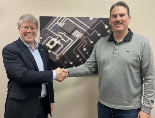
Images courtesy of APES Subscribe to Our Email Newsletter Stay up-to-date on all the latest news from the 3D printing industry and receive information and offers from third party vendors.Print Services Upload your 3D Models and get them printed quickly and efficiently.Powered by FacFox Powered by 3D Systems Powered by Craftcloud Powered by Xometry 3DPrinting Business Directory 3DPrinting Business Directory
Read More